Detect Radiation with Semiconductor Material
We offer our customers in the world outstanding products and services for their radiation detector applications
Inspired by photons!
NEWS
- On June 26, 2025, ijsmart received the Certificate of Venture Company from the Ministry of SMEs and Startups (MSS)
- Our CdZnTeSe detector perperformance was presented at 2024 IEEE NSS-MIC-RTSD Conference. Detailed information of presentation can be found from link
R-05-02 The mobility-lifetime product of holes in CdZnTeSe depending on Se contents
What is Cadmium Zinc Telluride Selenide (CdZnTeSe) ?
CdZnTeSe is recently updated semiconductor detector material operating at room-temperature.
CdZnTeSe detector is ideal solution for medical imaging, industrial applications, and homeland security due to its
high sensitivity for X-and gamma-ray and high count rate (> 107 photons/mm2/s) capability without polarization effect. In CdTe compounds, the difference between the mobility-lifetime product of electrons and holes varies by a factor of 100 more. Thus, charge carriers (mainly holes) generated by incident photons are trapped at defects on the way to the elctrode, and trapped charges form localized space charges, which can cause polarization effects and deviation of the internal E-field.
The number of trapped charges causing polarization is most pronounced in high-flux condictions such as medical and synchrotron applications. Therefore, improvement of hole transport properties is essential for these high flux applications.
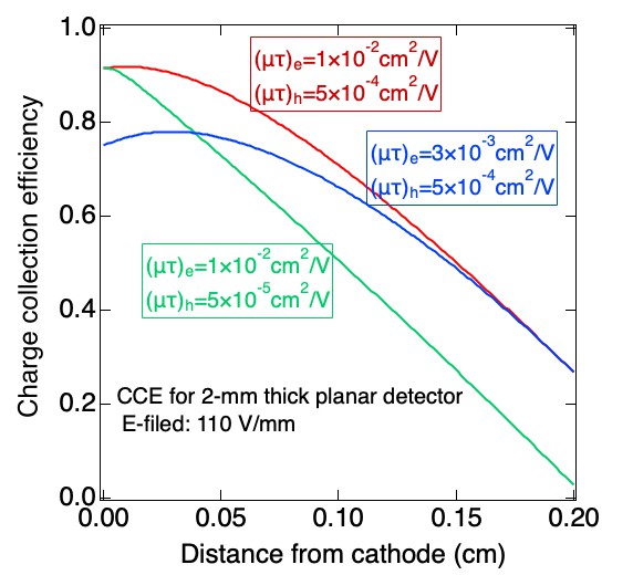
- In CdZnTeSe detector, mobility-lifetime product of electrons and holes are > 3 x 10⁻³ cm2/V and > 1 x 10⁻⁴ cm2/V, respectively. The contribution of holes on the charge collection efficiency (CEE) for 2-mm planar detector becomes important when the ratio of the mobility-lifetime product of holes and electrons is larger than 0.1 (see figure).
- Etch pit densities (EPDs) are less than 104 / cm2.
- Average Te incluions larger than 10 um is less than 3000 /cm2.
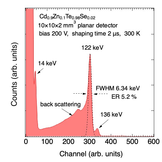
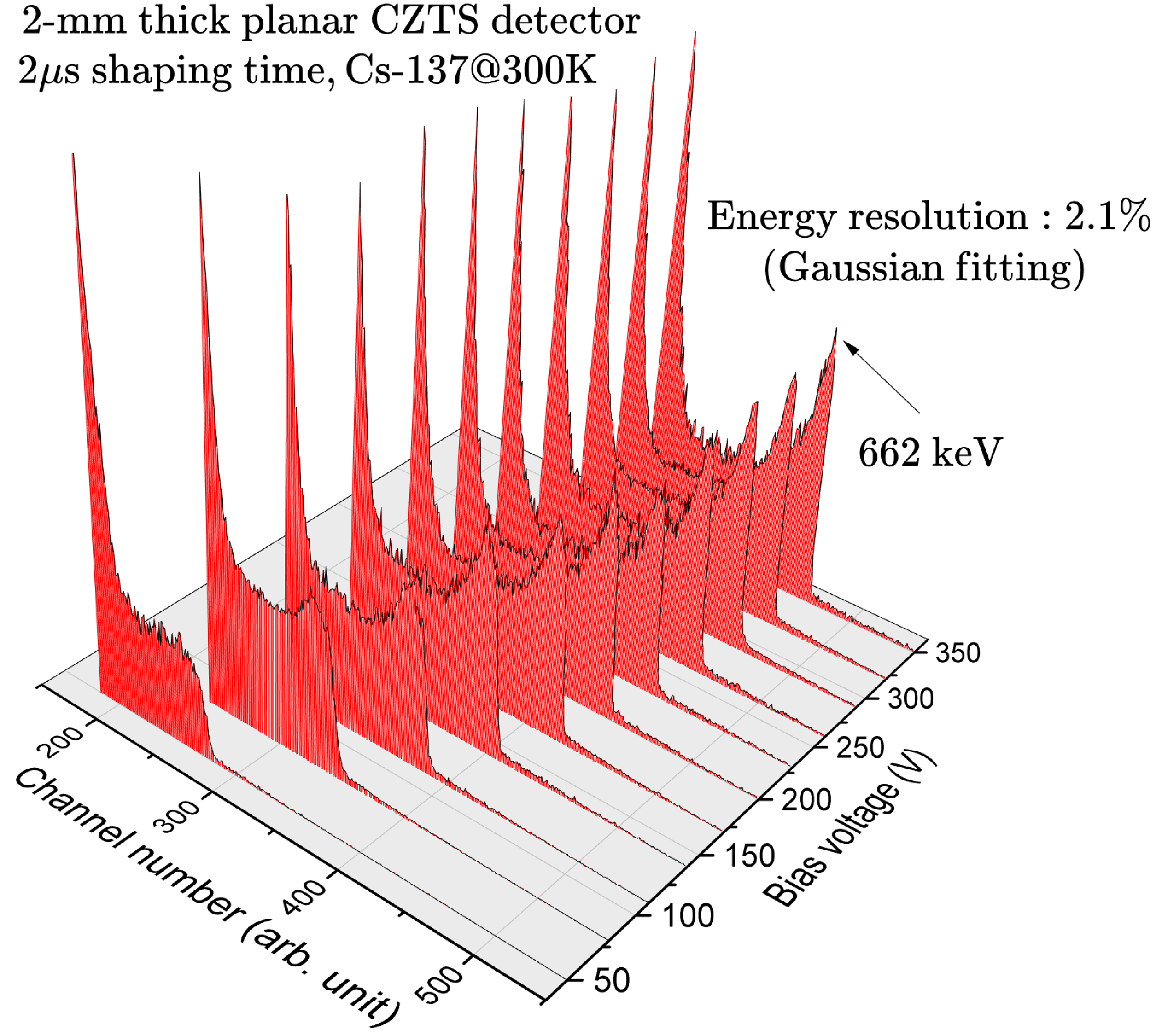
- Pulse height spectra of Co-57 and Cs-137 taken with 2-mm thick planar CZTS detector (see figure) exhibit excellent detection performance with high energy resolution due to the enhanced charge collection efficiency.
- Enhanced hole mobility-lifetime product in selenium-added CdTe compounds
- Evaluation of CdZnTeSe as a high-quality gamma-ray spectroscopic material with better compositional homogeneity and reduced defects
Related Publication List
Applications of Semiconductor-based Radiation Detector!
Traditional radiation spectrometers have poor energy resolution and non-portable due to cryogenic cooling system. However, wide bandgap CdTe-based semiconductor radiation detector (ex, CdZnTe, CdMnTe, CdZnTeSe, CdMnTeSe) can operate in room-temperature withoug cooling and can provide high energy and spatial resolution. Application area is as follows
- SPECT, PET and CT scanners (Especially, Photon Counting Computed Tomography (PCCT))
- Bone densitometers
- Medical probes
- Nonproliferation of nuclear materails
- Safeguards measurements: custom inspection systems, radiation monitoring for nuclear safeguard
- Secondary inspection for portals
- Nuclear waste management
- X-ray and gamma-ray cameras
- XRF material analyses
- Environmental radioactivity monitoring
- Gamma-Ray Spectroscopy
- Synchrotron X-ray research
Provide CdTe-based compounds material in forms of the ingot, wafer, and detector.
2-inch diameter CdTe-based compounds (such as CdZnTeSe, CdZnTe, and CdMnTe) ingots are grown by seedless travelling heater method (THM) and Bridgman method.
- 2-inch diameter wafer (wafer thickness : 11 mm)
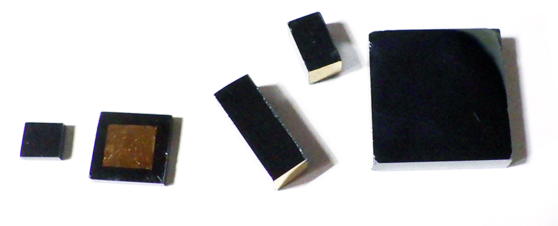
- Standard planar detector: 5 x 5 x 2 mm3, 5 x 5 x 5 mm3, 10 x 10 x 2 mm3 , and 20 x 20 x 5 mm3
- Standard bar-type detector : 6 x 6 x 12 mm3 (ER < 2 % for 662 keV)
- Standard hemi-spherical detector : 5 x 5 x 3 mm3, 10 x 10 x 5 mm3 (ER < 3 % for 662 keV)
- Custom size detector available on request